


01
Deep PDK Expertise
Extensive experience in PDK development, physical verification and sign-off methodologies across multiple process generations.

SiliconGrid provides comprehensive PDK development and verification services across planar, FinFET, GAA, and advanced packaging technologies—
from sign-off rule decks and parasitic extraction to QA and production readiness.


01
Extensive experience in PDK development, physical verification and sign-off methodologies across multiple process generations.
02
Rigorous QA methodologies designed to improve release quality.
03
Engineering capabilities spanning planar, FinFET, GAA and advanced packaging technologies.
04
Hands-on engineering focused on real design-rule behavior, tool compatibility and production usability.

Comprehensive PDK development and quality assurance - delivering reliable sign-off quality across advanced process nodes.
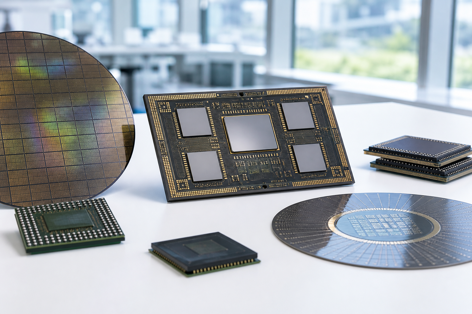
PDK development and verification methodologies for 2.5D interposer, 3D chiplet, and fan-out packaging technologies, enabling reliable heterogeneous integration.
COPYRIGHT 2026(C) SiliconGrid. ALL RIGHTS RESERVED. DESIGNED BY WEBSITE.CO.KR
